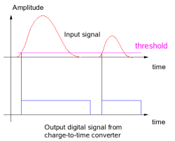
Figure 1: Measurement of charge of a signal with charge-to-time conversion.
Front-End Electronics for a GEM TPC based on TDC
Working Principle
The main idea of the readout electronics based on Time-to-Digital Converters (TDC) is to measure the charge of the signal from a TPC with the help of a charge-to-time converter(QTC). The digital pulse on the output of the QTC represents the charge of the signal on the analog input. The larger signal on the input - the longer pulse duration of the signal on the output of the QTC, Figure 1.
The time of arrival of a signal is obtained at the moment of time when the leading edge of the signal crosses a threshold potential. This automatically performs "zero data" suppression. Thus, information on charge of the signal and its arrival time are effectively encoded into time information. Signals from QTC are digitized with a Time-to-Digital Converter. Together, QTC and a TDC compose a Wilkinson-type ADC.
One of the important parameters of such ADC is the maximum conversion time: a time interval required to encode the largest signal (within QTC range). Charge-to-time converters which produce long pulses relax requirement on TDC time resolution, but double pulse resolution of a readout system degrades.
In the TPC applications, it is more important to measure small signals (due to charge sharing between pads), rather than very large signals (large energy deposits due to ionization fluctuation). In this case a logarithmic charge-to-time conversion characteristic becomes attractive.
Front-End Electronics
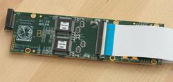
A Front-End Electronics (FEE) board for the Large Prototype TPC uses 4 ASDQ chips, Figure 2. Each 8-channel chip performs amplification, shaping, and measurement of the charge of the signals. The size a 32-channel readout electronics board is 106 mm * 30 mm. The thickness of a board is 4.4 mm. The area occupied by a board (4.4 mm * 30 mm) allows to work with pad sizes as small as (~1 mm * 4 mm). The boards are connected directly to a GEM Module. Short path between the TPC pads and readout electronics reduces the pick-up noise.
Signals from a FEE board transmitted via 20 cm long flat flexible cables to a cable Pitch Adapter. The function of the Pitch Adapter is to connect fine-pitch flexible cable to twisted pair cables, which are connected to commercial VME TDCs.
In total there are 28 readout boards available. Since there are only 5 TDC modules available (a single TDC module has 128 channels), only 20 boards to be used for tests.
Test equipment
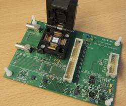
The prototype of the readout system - the "Chip Tester" board has served not only as a prototype of the readout system, where many design principles were tested, but also helped to test and select ASDQ chips, Figure 3. Procedure of selection included following steps:
- optical inspection
- check of power consumption
- counting signals with TDC
- analysis of time and charge measurements for a defined condition on the input
- 164 out of 200 chips fulfilled criteria on uniformity of the time and charge measurement
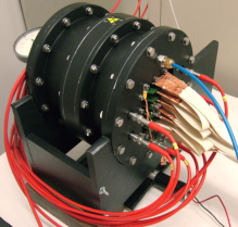
In order to test readout electronics in more realistic environment, a small test chamber UNIMOCS (UNIversal MOdular Chamber System) has been build, Figure 4. The chamber is based on a triple GEM setup with 3 cm drift gap. It features no field cage, since the inhomogeneities of the electric field in the drift gap are of no concern. Absence of the field cage also simplifies the design of the chamber. The UNIMOCS features interchangeable pad-plans, so that readout electronics with different connectors can be tested. In the next step, the readout electronics will be tested with the Large Protoype TPC.
More information about this electronics can be found on the webpage about TDC electronics
development (Rostock University / DESY) and in the following EUDET memos:
- EUDET-Memo-2008-39: Status of TPC-electronics with Time-to-Digit Converters
- EUDET-Memo-2008-05: A Prototype for TDC-based Readout Electronics for the LP TPC
- EUDET-Memo-2007-38: Status Report on TDC-based readout electronics for the LP TPC.
- EUDET-Memo-2006-02: Status of the R&D Program for a Read-Out System based on Time to Digital converters for the LC-TPC within EUDET


